

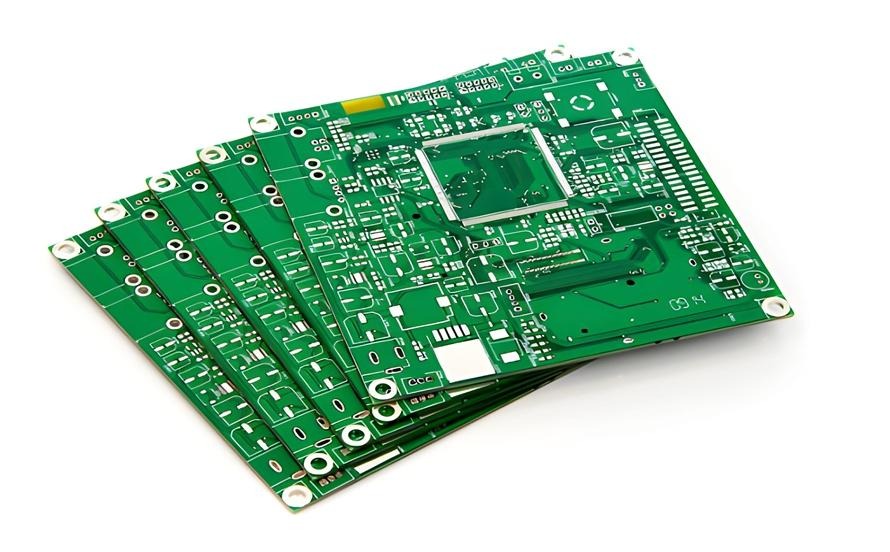
The accuracy of electronic assembly plays a crucial role in determining the performance, reliability, and longevity of every printed circuit board. While much attention is often given to PCB design and fabrication, one essential component of the assembly process is frequently overlooked—the PCB Stencil. This precision-engineered tool is responsible for applying solder paste accurately to the printed circuit board before surface mount components are placed, making it one of the most important elements in modern electronics manufacturing.
As electronic devices continue to become smaller and more complex, the demand for precise solder paste deposition has increased significantly. Fine-pitch components, Ball Grid Arrays (BGAs), Quad Flat No-lead (QFN) packages, and miniature passive devices require highly accurate stencil designs to ensure reliable solder joints. Even slight inconsistencies during solder paste application can result in assembly defects that affect product quality and increase manufacturing costs.
Many USA PCB Manufacturers provide complete PCB manufacturing and assembly solutions, including stencil design and production, to ensure consistent assembly quality. Their investment in precision manufacturing equipment and advanced quality control enables companies to produce reliable electronic products for industries with demanding performance requirements.
This article explores the importance of PCB stencils, how they are manufactured, their role in PCB assembly, key advantages, applications, and why experienced USA PCB manufacturers remain trusted partners for electronics production.
What Is a PCB Stencil?
A PCB Stencil is a thin sheet of stainless steel or other specialized material that contains precisely laser-cut openings corresponding to the solder pads on a printed circuit board. During PCB assembly, the stencil is positioned over the board, allowing solder paste to be applied only where electronic components will be mounted.
Once the solder paste is deposited through the stencil openings, surface mount components are placed onto the board using automated pick-and-place equipment. The board then passes through a reflow oven, where the solder paste melts and forms permanent electrical and mechanical connections between the components and the PCB.
The accuracy of the stencil directly influences solder joint quality, component alignment, and overall assembly reliability. For modern high-density circuit boards, even microscopic variations in stencil dimensions can significantly affect production quality.
Why PCB Stencils Are Essential
The primary function of a PCB Stencil is to ensure consistent solder paste deposition across every production board. Accurate solder volume is critical because too much solder can create bridges between adjacent pads, while too little solder may result in weak or incomplete electrical connections.
Modern electronic assemblies often include extremely small components with minimal spacing between solder pads. These designs require highly precise stencil apertures that deliver uniform solder paste volumes throughout the production process.
Consistent solder deposition also improves manufacturing efficiency by reducing assembly defects and minimizing manual rework. Higher first-pass yields translate into lower production costs and improved product reliability.
As electronic products become increasingly sophisticated, precision stencil manufacturing has become a key factor in supporting reliable high-volume PCB assembly.
The PCB Stencil Manufacturing Process
The production of a PCB Stencil begins with PCB design data that identifies every solder pad requiring paste deposition. Engineers analyze component sizes, pad geometries, solder paste characteristics, and assembly requirements before optimizing the stencil aperture design.
High-quality stainless steel sheets are commonly selected because they offer excellent dimensional stability, durability, and resistance to repeated cleaning cycles. Advanced laser cutting systems create highly accurate stencil openings with extremely tight tolerances suitable for fine-pitch electronic assemblies.
Following laser cutting, the stencil surface is polished to remove burrs and improve solder paste release during printing. Some manufacturers apply specialized nano-coatings that reduce solder paste adhesion, allowing cleaner and more consistent printing throughout extended production runs.
After dimensional verification and inspection, the completed stencil is mounted within a rigid frame or supplied as a frameless stencil, depending on the customer’s printing equipment and production requirements.
Advantages of High-Quality PCB Stencils
A precision PCB Stencil significantly improves solder paste accuracy, which directly contributes to higher assembly quality and product reliability. Uniform paste deposition helps create strong, consistent solder joints across every component on the board.
Another important advantage is improved manufacturing efficiency. Accurate stencil printing reduces solder defects such as bridging, insufficient solder, tombstoning, and void formation, minimizing production interruptions and costly rework.
High-quality stencils also support increasingly complex PCB designs. Fine-pitch integrated circuits, micro BGAs, QFN packages, and miniature passive components require precise aperture dimensions that only advanced stencil manufacturing can consistently achieve.
Durability is another major benefit. Stainless steel stencils withstand thousands of printing cycles while maintaining dimensional accuracy, making them suitable for both prototype production and high-volume manufacturing.
Additionally, optimized stencil designs contribute to improved production consistency by delivering repeatable solder paste deposition throughout extended manufacturing runs.
Applications of PCB Stencils
The PCB Stencil is an essential tool in virtually every surface mount assembly process. Consumer electronics manufacturers depend on precision stencils to assemble smartphones, laptops, tablets, wearable devices, gaming systems, networking equipment, and smart home products that contain densely populated circuit boards.
Automotive electronics manufacturers utilize precision stencil technology for engine control modules, electric vehicle battery management systems, advanced driver assistance systems, infotainment platforms, lighting controllers, and safety electronics that require highly reliable solder joints.
Medical device manufacturers rely on accurately manufactured stencils when assembling patient monitoring equipment, diagnostic instruments, imaging systems, laboratory analyzers, portable healthcare devices, and implantable medical electronics where assembly quality is critical.
Industrial automation equipment, aerospace electronics, defense systems, telecommunications infrastructure, renewable energy products, robotics, scientific instruments, and Internet of Things devices also require precision stencil printing to achieve dependable assembly performance.
Why USA PCB Manufacturers Continue to Be Trusted
Many USA PCB Manufacturers have earned strong reputations by providing high-quality PCB fabrication, assembly, and stencil manufacturing services supported by advanced engineering expertise and strict quality standards. Their close collaboration with customers helps ensure that stencil designs are optimized for the specific PCB layout, component package types, and assembly process.
Manufacturers in the United States often invest in state-of-the-art laser cutting systems, automated solder paste inspection equipment, advanced surface mount production lines, automated optical inspection, X-ray inspection, and functional testing technologies. These capabilities help maintain consistent quality while supporting highly complex electronic products.
Many companies also provide complete manufacturing solutions that include PCB design support, Design for Manufacturability analysis, prototype fabrication, PCB assembly, stencil production, testing, and supply chain management. This integrated approach improves communication between design and manufacturing teams while reducing production lead times.
For industries such as aerospace, defense, medical devices, industrial automation, and telecommunications, domestic manufacturing also provides greater supply chain transparency, technical collaboration, and compliance with industry-specific regulations.
Quality Assurance in PCB Stencil Manufacturing
Quality assurance is fundamental to producing a reliable PCB Stencil because stencil accuracy directly influences assembly performance. Manufacturers begin by verifying customer design data and confirming aperture dimensions before production begins.
During manufacturing, laser cutting systems are carefully calibrated to maintain precise opening dimensions and smooth aperture walls. After cutting, stencils undergo detailed dimensional inspection using high-resolution optical measurement systems to verify compliance with engineering specifications.
Surface quality is also evaluated to ensure efficient solder paste release during printing. Additional inspections may include flatness measurement, frame alignment verification, thickness confirmation, and aperture accuracy analysis.
Once the stencil enters production, manufacturers often use solder paste inspection systems to verify printing consistency while Automated Optical Inspection and X-ray analysis evaluate solder joint quality after component placement and reflow.
Leading manufacturers maintain internationally recognized certifications such as ISO 9001, IPC standards, UL compliance, ISO 13485 for medical electronics, IATF 16949 for automotive manufacturing, and AS9100 for aerospace applications. These quality systems ensure that both stencil production and PCB assembly consistently meet the demanding requirements of modern electronics manufacturing.
Conclusion
The PCB Stencil is a critical component of the surface mount assembly process, enabling accurate solder paste deposition that directly influences product quality, manufacturing efficiency, and long-term reliability. As electronic products continue to evolve toward higher component density and greater complexity, precision stencil manufacturing has become more important than ever.
Leading USA PCB Manufacturers continue to support global electronics innovation through advanced stencil production, high-quality PCB fabrication, and comprehensive assembly services. Their investment in precision manufacturing technologies, engineering expertise, and rigorous quality assurance enables businesses to produce reliable electronic products for industries ranging from consumer electronics and industrial automation to healthcare, automotive, aerospace, and telecommunications. By selecting an experienced manufacturing partner, companies can improve assembly quality, reduce production risks, and accelerate the successful launch of advanced electronic products.
