
The electronics industry has undergone significant changes over the past two decades as manufacturers have adopted environmentally responsible production practices. One of the most important developments has been the transition from traditional lead-based soldering materials to safer alternatives. This shift has led to the widespread adoption of lead free PCB assembly, a manufacturing process that eliminates the use of lead in soldering while maintaining the reliability and performance required by modern electronic products.
Today, lead-free manufacturing has become the standard for many industries, driven by environmental regulations, consumer demand for sustainable products, and advancements in soldering technology. From consumer electronics and medical devices to automotive systems and industrial equipment, lead free PCB assembly plays a critical role in producing high-quality electronic products while reducing environmental impact.
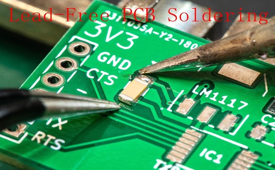
What Is Lead Free PCB Assembly?
Lead free PCB assembly is the process of manufacturing printed circuit board assemblies using solder alloys that do not contain lead. In traditional electronics manufacturing, solder materials often consisted of a mixture of tin and lead, which provided reliable electrical connections and relatively low melting temperatures.
However, concerns about the environmental and health risks associated with lead exposure prompted the industry to develop alternative solder materials. Lead-free solder typically consists of tin combined with metals such as silver, copper, bismuth, or other elements that provide suitable mechanical and electrical properties.
During lead free PCB assembly, all soldering processes, including surface mount technology and through-hole assembly, utilize these lead-free materials. The result is a finished electronic assembly that complies with modern environmental standards while delivering dependable performance.
Why the Industry Moved Toward Lead-Free Manufacturing
The primary reason for adopting lead free PCB assembly is the reduction of environmental and health risks associated with lead. Lead is a toxic heavy metal that can accumulate in soil, water, and living organisms if not properly managed.
As electronic waste volumes increased worldwide, governments and regulatory organizations introduced restrictions on hazardous substances used in electronic products. These regulations encouraged manufacturers to eliminate lead and other potentially harmful materials from their production processes.
The transition to lead-free technology has helped reduce the environmental impact of electronics manufacturing and disposal. It has also improved workplace safety by minimizing exposure to hazardous substances during production.
Today, many global markets require compliance with environmental standards that support lead-free manufacturing practices.
Understanding Lead-Free Solder Alloys
The success of lead free PCB assembly depends largely on the development of effective solder materials that can replace traditional tin-lead alloys. Several lead-free formulations have become widely accepted throughout the electronics industry.
One of the most common lead-free solder compositions combines tin, silver, and copper. This alloy offers strong mechanical performance, good electrical conductivity, and reliable solder joint formation.
Other formulations may include bismuth, antimony, or nickel to enhance specific performance characteristics. The selection of a particular solder alloy depends on factors such as product requirements, operating environment, reliability expectations, and manufacturing processes.
Although lead-free solders generally require higher processing temperatures than traditional solder materials, advancements in manufacturing technology have made their implementation highly successful across a wide range of applications.
The Lead Free PCB Assembly Process
The lead free PCB assembly process follows many of the same manufacturing principles used in conventional PCB assembly. However, certain process parameters must be adjusted to accommodate the unique properties of lead-free solder materials.
The process begins with solder paste application. Lead-free solder paste is printed onto designated PCB pads using precision stencil equipment. Accurate solder deposition is essential for creating reliable electrical connections.
Next, automated pick-and-place machines position electronic components onto the board. Modern assembly systems ensure precise placement regardless of component size or complexity.
The board then enters a reflow soldering oven where carefully controlled temperature profiles melt the lead-free solder and form permanent connections. Because lead-free alloys typically have higher melting points, reflow temperatures are generally higher than those used with traditional lead-based solder.
Following soldering, inspection and testing procedures verify assembly quality and functional performance.
Advantages of Lead Free PCB Assembly
One of the most significant benefits of lead free PCB assembly is environmental sustainability. By eliminating lead from electronic products, manufacturers contribute to safer disposal practices and reduced environmental contamination.
Lead-free solder alloys also provide excellent mechanical strength and durability. In many applications, these materials offer improved resistance to thermal fatigue and mechanical stress compared to traditional lead-based solder.
Compliance with international regulations represents another important advantage. Many markets require lead-free manufacturing to meet environmental standards and facilitate global product distribution.
Additionally, lead-free technology supports corporate sustainability initiatives and enhances a company’s reputation among environmentally conscious customers and stakeholders.
These benefits have made lead-free assembly the preferred manufacturing approach for many electronics producers.
Challenges in Lead Free PCB Assembly
Despite its advantages, lead free PCB assembly presents several manufacturing challenges. One of the most notable differences is the higher processing temperature required by lead-free solder materials.
Elevated temperatures can place additional stress on components and PCB materials, requiring careful process control to prevent damage. Manufacturers must optimize reflow profiles and thermal management strategies to ensure reliable assembly outcomes.
Lead-free solders may also exhibit different wetting characteristics compared to traditional alloys. Achieving consistent solder joint quality often requires precise control of solder paste formulation, stencil design, and process parameters.
In addition, equipment used for lead-free production must be properly maintained and calibrated to support the more demanding thermal requirements of these materials.
Addressing these challenges requires specialized expertise and manufacturing experience.
Quality Control in Lead Free PCB Assembly
Quality assurance is essential for maintaining reliability in lead free PCB assembly. Manufacturers implement comprehensive inspection and testing procedures throughout the production process.
Automated Optical Inspection systems evaluate component placement accuracy, solder joint quality, and assembly integrity. These inspections help identify defects before products proceed to final testing stages.
X-ray inspection is often used for advanced semiconductor packages where solder joints are not visible externally. This technology provides detailed images that reveal hidden defects and connection issues.
Electrical testing methods such as In-Circuit Testing and functional testing verify product performance and ensure compliance with design specifications.
By combining advanced inspection technologies with rigorous process controls, manufacturers can achieve high-quality lead-free assemblies that meet industry standards.
Applications of Lead Free PCB Assembly
Lead free PCB assembly is widely used across nearly every segment of the electronics industry. Consumer electronics manufacturers rely on lead-free processes for smartphones, tablets, laptops, gaming systems, and smart home devices.
Automotive companies use lead-free assemblies in engine control systems, infotainment units, sensors, battery management systems, and electric vehicle technologies. Medical device manufacturers also depend on lead-free manufacturing to support regulatory compliance and patient safety.
Industrial automation systems, telecommunications equipment, aerospace electronics, renewable energy products, and Internet of Things devices all benefit from lead-free assembly technologies.
The broad adoption of lead-free manufacturing reflects its importance in supporting modern electronics production worldwide.
The Future of Lead Free PCB Assembly
As environmental awareness continues to grow, lead free PCB assembly is expected to remain the dominant manufacturing approach in the electronics industry. Research into new solder materials and process technologies is helping improve reliability, performance, and manufacturing efficiency.
Advanced automation systems, artificial intelligence, and real-time process monitoring are further enhancing quality control capabilities. These innovations help manufacturers maintain consistent production standards while reducing waste and improving sustainability.
Future developments may introduce new lead-free materials with enhanced thermal and mechanical properties, supporting increasingly demanding electronic applications.
As electronic products continue to evolve, lead-free manufacturing will remain a key component of responsible and sustainable production practices.
Conclusion
Lead free PCB assembly has become an essential part of modern electronics manufacturing, providing a safer and more environmentally responsible alternative to traditional lead-based soldering processes. By utilizing advanced lead-free solder alloys, optimized manufacturing techniques, and comprehensive quality control procedures, manufacturers can produce reliable electronic assemblies that meet both performance requirements and environmental regulations. From consumer electronics and automotive systems to medical devices and industrial equipment, lead-free technology supports a wide range of applications while reducing environmental impact. As sustainability and regulatory compliance continue to influence global manufacturing practices, businesses increasingly rely on an experienced lead free PCB assembly service provider to deliver high-quality, compliant, and dependable electronic products for today’s competitive markets.