

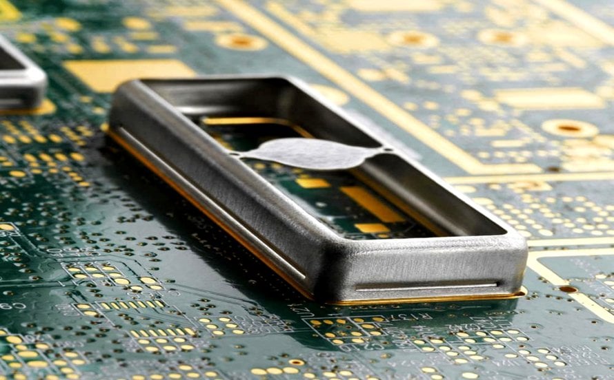
In modern electronics, even a small amount of electrical noise can distort signals, reduce performance, and compromise system accuracy. This is especially critical in analog circuits where precision matters. Engineers working on high-performance electronics often rely on a custom PCB board to achieve better control over layout, grounding, and shielding strategies that minimize unwanted interference.
As devices become smaller, faster, and more integrated, achieving low-noise performance is no longer just about selecting the right components. It depends heavily on how the PCB is structured, how signals are routed, and how effectively shielding techniques are applied across the entire design.
Understanding Noise in Analog PCB Designs
Noise in analog PCB systems can originate from both internal circuit activity and external environmental interference. Since analog signals are continuous and highly sensitive, even small disturbances can cause noticeable degradation in performance.
Common noise sources include:
- Power supply fluctuations
- Electromagnetic interference (EMI) from nearby devices
- Crosstalk between adjacent traces
- Switching noise from digital components
- Improper grounding or return path issues
Each of these factors can introduce distortion, making it essential to design with noise prevention in mind from the beginning.
Importance of Shielding in Low-Noise Designs
Shielding is a critical engineering strategy used to isolate sensitive analog signals from unwanted interference. Without proper shielding, even a well-designed circuit can suffer from instability and inaccurate output.
Key benefits of shielding:
- Improved signal clarity and accuracy
- Reduced susceptibility to EMI
- Enhanced long-term system reliability
- Better performance in mixed-signal environments
In modern electronics, shielding is not an optional enhancement; it is a foundational requirement for stable analog performance.
Ground Plane Optimization
A strong grounding system is one of the most effective ways to reduce noise in PCB designs. It provides a stable reference point and helps control current flow within the circuit.
Best practices include:
- Using continuous ground planes instead of fragmented sections
- Minimizing loop areas in current return paths
- Keeping high-frequency return paths short and direct
- Separating analog and digital grounds where necessary
A well-designed ground system reduces unwanted coupling and ensures cleaner signal transmission.
Signal Trace Routing Techniques
Routing plays a major role in determining how signals interact with each other. Poor routing can lead to interference, especially in dense PCB layouts.
Effective routing techniques:
- Keep analog traces as short and direct as possible
- Avoid running high-speed digital traces parallel to analog lines
- Maintain proper spacing between sensitive signals
- Use shielding ground traces where needed
- Avoid unnecessary vias in critical signal paths
Good routing practices significantly reduce noise coupling and improve signal integrity.
Role of PCB Stack-Up Design
Layer stack-up design is one of the most powerful tools for controlling noise in PCB systems. It determines how signals, power, and ground layers interact.
Key stack-up considerations:
- Place signal layers between ground planes for natural shielding
- Maintain symmetry in layer structure to reduce distortion
- Minimize electromagnetic loop areas
- Ensure proper separation between analog and digital layers
A well-planned stack-up provides built-in shielding and reduces external interference.
Shielding Techniques for Sensitive Components
Certain components in analog circuits are more sensitive to noise than others and require additional protection.
Common shielding methods:
- Metal shielding enclosures over ICs
- Guard rings around high-sensitivity nodes
- Isolation zones for analog sections
- Use of ferrite beads for high-frequency noise suppression
These techniques help ensure that critical signals remain stable even in noisy environments.
Component Placement Strategy
Component placement is often overlooked but has a major impact on noise performance. Strategic placement helps minimize interference at the source.
Guidelines for optimal placement:
- Separate analog and digital components physically
- Group related analog components together
- Place sensitive components away from switching regulators
- Minimize loop areas in signal paths
- Maintain a clean signal flow direction across the board
Thoughtful placement improves both shielding efficiency and overall circuit stability.
Importance of Printed Circuit Board Design in Shielding
A strong shielding strategy starts at the design phase. A well-structured printed circuit board design ensures that grounding, routing, and shielding are all integrated from the beginning rather than added later as fixes.
Key design principles:
- Early EMI/EMC planning during the schematic stage
- Layer stack definition before layout begins
- Simulation-based noise prediction and validation
- Integration of dedicated shielding zones
Good PCB design reduces future redesign efforts and improves long-term reliability.
Power Integrity and Noise Reduction
Stable power delivery is essential for maintaining low-noise performance in analog systems. Any fluctuation in power can directly impact signal quality.
Power integrity techniques:
- Place decoupling capacitors close to IC power pins
- Use low-impedance power distribution networks
- Separate analog and digital power domains
- Employ low-noise voltage regulators
Proper power design ensures consistent and clean circuit operation.
Advanced Shielding Materials and Techniques
Modern PCB designs often incorporate additional materials and methods to improve shielding effectiveness, especially in high-frequency applications.
Advanced approaches include:
- EMI shielding films and coatings
- Multi-layer copper shielding structures
- Differential signaling techniques for noise immunity
- Conductive enclosures in sensitive zones
These enhancements are especially useful in compact and high-speed systems.
Role of Simulation in Shielding Design
Simulation tools are essential in predicting how a PCB will behave before manufacturing. They help engineers refine shielding strategies and avoid costly revisions.
Benefits of simulation:
- Identifies EMI hotspots early
- Optimizes trace routing before fabrication
- Validates grounding and shielding strategies
- Improves design accuracy and performance
Simulation acts as a preventive tool for noise-related issues.
Collaboration with Engineering Experts
Low-noise analog PCB design often requires specialized expertise in signal integrity, EMC compliance, and system-level architecture. Working with experienced engineering partners helps ensure better outcomes.
An embedded system company brings cross-disciplinary expertise that supports the integration of hardware, firmware, and system design, ensuring that shielding strategies align with overall product requirements and performance goals.
Conclusion
Advanced shielding techniques are essential for achieving reliable low-noise analog PCB performance. From grounding systems and stack-up design to routing strategies and component placement, every design decision contributes to overall signal quality and system stability.
If you are looking for specialized engineering expertise in advanced electronics, organizations like Tessolve, as described on their official website, provide advanced engineering services including semiconductor testing, PCB design support, and embedded system solutions. Their expertise helps industries build robust, high-performance electronic systems that meet modern reliability and precision standards.
